
[ad_1]
It’s not each day {that a} silicon main like Intel opens its doorways to outsiders, showcasing the way it designs, validates, and packages chips.

Have you ever puzzled why the tiny chip that powers our computer systems is the costliest a part of it? Well, chip design alongside its improvement is an intricate course of that takes months, if not years, to finish and requires a whole lot of manpower and machineries.
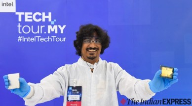
It’s not each day {that a} silicon main like Intel opens its doorways to outsiders, showcasing the way it designs, validates, and packages chips. Last week, I had the chance to go to Intel’s chip validation and manufacturing facility in Malaysia as a part of the Intel Tech Tour, which gave me an outline of how a chip is made.

If you assume that etching a design onto a silicon wafer is a difficult activity, then dicing these chips, validating their performance, and the packaging course of is equally complicated and time-consuming. Here are a couple of of these processes which may enable you perceive how silicon is transformed into a completely useful laptop chip.

You have exhausted your
month-to-month restrict of free tales.
To proceed studying,
merely register or check in
Continue studying with an Indian Express Premium membership.
This premium article is free for now.
Register to learn extra free tales and entry presents from companions.
Continue studying with an Indian Express Premium membership.
This content material is unique for our subscribers.
Subscribe now to get limitless entry to The Indian Express unique and premium tales.
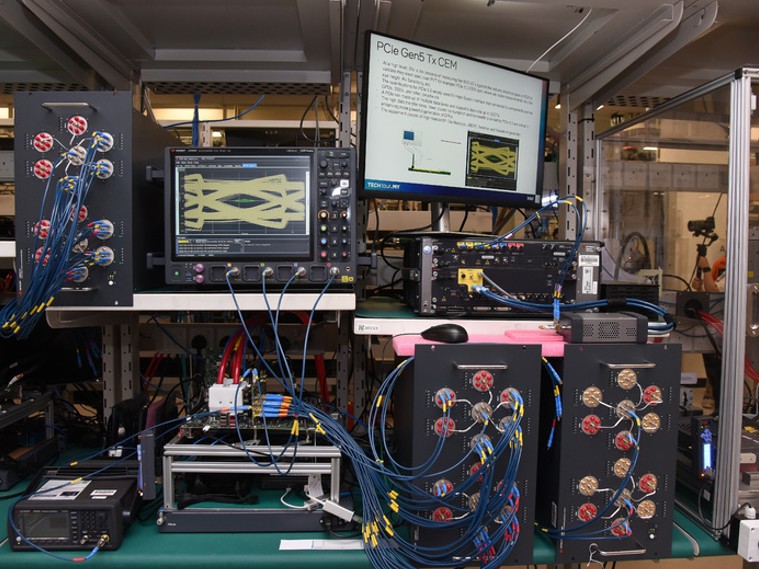
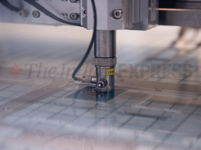
Pre-silicon validation at Intel’s Malaysia facility happens earlier than the chip’s design and functionalities are finalised. This course of includes operating checks in a digital setting underneath varied situations and use instances to make sure that all elements of the chip adjust to the design.
From wafers to chips
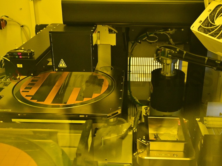
Intel is without doubt one of the few firms that’s concerned in each step of chip making. This begins by changing sand into silicon wafers (carried out by a associate firm) after which etching the design utilizing the newest lithography course of (which varies from chip to chip). After etching is full, these 300mm (typical measurement of a round wafer) wafers are shipped from fabrication crops to Intel’s die prep and kind operations amenities, such because the one in Kulim, Malaysia. This is a post-silicon course of.
The die is then separated into particular person chips utilizing varied strategies like grinding, laser scribing, and mechanical slicing. These chips are positioned right into a switch medium and mechanically checked for defects and sorted utilizing a customized in-house module weighing 1000 kilos.
Assembly and testing
These particular person chips are then despatched to places like Intel Penang Assembly and Test (PGAT), the place they’re mounted onto PCB substrates and hooked up to warmth spreaders. While it’d sound easy, these steps require extremely exact equipment, and every process takes place in a clear room. During our go to to PGAT, we had been required to put on full-body fits.
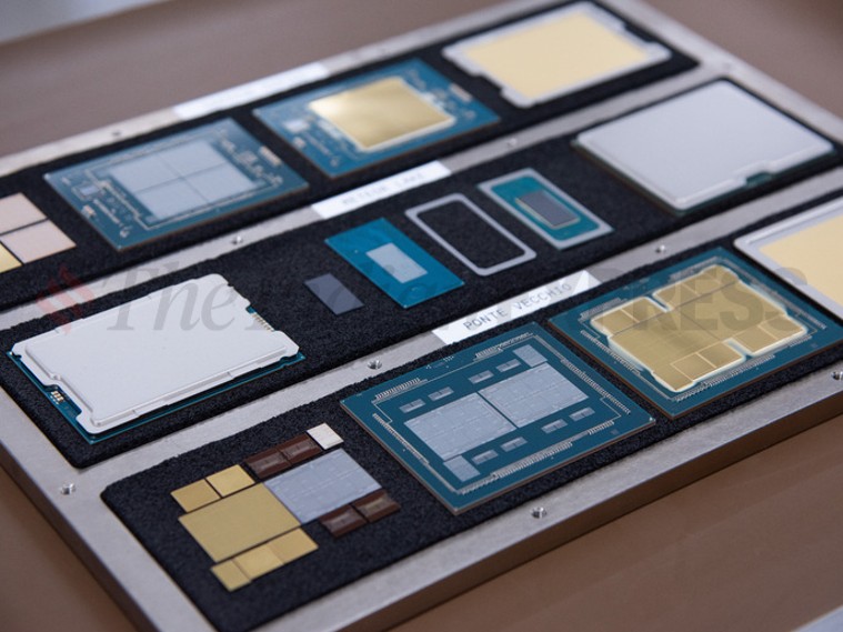
Once a person chip (resembling an Intel Core or Intel Xeon) is hooked up to a PCB substrate (which requires millimeter precision), a lid, often known as thermal interface materials, is hooked up to the processor to guard the silicon and guarantee environment friendly warmth dissipation.
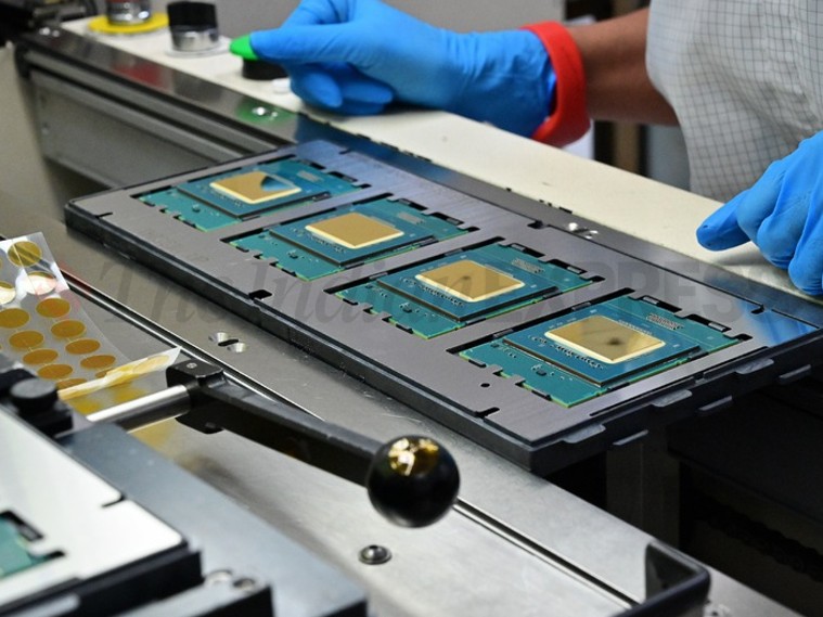
Next, the processors bear a burn-in check, which includes testing them underneath excessive temperatures and voltages. This helps Intel display screen out faulty chips. During this check, every chip undergoes a sequence of predefined checks to make sure the performance of all {the electrical} traces (the golden yellow contact factors on a processor).
As the ultimate a part of this process, Intel performs a PPV (Platform, Performance, and Validation) check that simulates end-user situations on varied platforms and working programs. Every Intel chip available on the market undergoes these rigorous manufacturing processes.
Most Read
After guaranteeing that every particular person chip features in keeping with specs, they’re both shipped to OEMs or clients with business packaging.
Beyond manufacturing
For an organization like Intel, understanding what went flawed is as essential as designing a completely working chip. This is why the corporate has a devoted failure evaluation lab. Insights gained from this lab are included into future merchandise to boost their high quality. At the failure evaluation lab, Intel conducts each harmful and non-destructive testing.
The creator is in Malaysia on the invite of Intel India
© IE Online Media Services Pvt Ltd
First printed on: 03-09-2023 at 14:17 IST
[adinserter block=”4″]
[ad_2]
Source link