[ad_1]
At the second, probably the most highly effective Arm processor on the planet is the 48-core A64FX processor from Fujitsu, which was created because the closely vectored compute engine for the “Fugaku” supercomputer at RIKEN Lab in Japan. Nvidia is on the brink of ship its 72-core “Grace” Arm CPU, which has but to be given a product title however CG100 appears logical. And each are going to be getting some intense competitors from a newcomer primarily based in India.
There is a non-zero probability that the Aum HPC processor designed by the Center for Development of Advanced Computing (C-DAC) might outperform each A64FX and Grace and even give Amazon’s 64-core Graviton3 chip and Ampere Computing’s Altra, Altra Max, and AmpereOne processors a run for the cash on extra generic workloads.
The particulars of the Aum HPC processor came to light this week, and couldn’t have come at a greater time as we’re only a tad bit sick of writing about AI and it’s fairly quiet on the market in IT Land regardless of this being the week earlier than the International Super Computing convention in Frankfort. The Aum HPC processor was developed below the auspices of the National Supercomputing Mission of the Indian authorities, and the presentation that we now have seen was put collectively by Sanjay Wandhekar, senior director of the HoD HPC Technologies Group at C-DAC.
The mission brings collectively the Indian Institute of Science, the Department of Science and Technology, the Ministry of Electronics and Information Technology, and C-DAC to carry HPC independence, from the processor all the best way as much as full methods and software program, to the federal government of India and the organizations that want HPC processing and, presumably, Indian trade giants who can also not need to be depending on exterior sources of silicon, methods, and software program for his or her HPC and AI workloads. This isn’t solely a know-how effort, but in addition a one regarding manufacturing in addition to datacenter design with an emphasis on liquid cooling for probably the most highly effective – and we presume exascale – equipment. The effort additionally contains creating supercomputing purposes “of national interest” and cultivating the programming and system administration experience essential to create these purposes, keep them, and run them in manufacturing.
In addition to having a provide chain for HPC components and methods that’s immune from attainable import into India, the Indian authorities can also be eager on understanding, indisputably, that there are not any safety backdoors within the {hardware} or software program it makes use of to deploy HPC and AI purposes. Given that India is a nuclear energy that shares a border with China and is however a stone’s throw away from Russia, it’s not onerous to grasp why India is embracing the Arm structure and doing a customized processor. And it won’t be stunning when Pakistan, which additionally shares a border with India and which has about the identical variety of nuclear weapons as India, does a customized processor, too. Perhaps it is going to be primarily based on RISC-V?
The Aum HPC processor isn’t restricted to the HPC market, and we will anticipate for variants of it for use within the AI and generic cloud computing areas as properly. The chip is predicted to be accessible in 2024, and will probably be initially deployed in a pilot HPC system with in extra of 1 petaflops of efficiency (presumably that is peak theoretical efficiency). After that, the Indian authorities is seeking to “be ready with exascale system design and subsystems” primarily based on the Aum CPU. (By the best way, we don’t assume the phrase “Aum” has something to do with “Arm,” however is an alternate spelling for “Om,” which is a romanization of an historical Sanskrit phrase that may be a sacred mantra within the Hindu religion.)
To create the Aum processor, the techies at C-DAC studied the A64FX processor and Fugaku system at RIKEN in addition to its predecessor Sparc64-VIIIfx processor and Okay supercomputer intensely noticed what all of us see within the HPCG benchmark knowledge. Getting a greater ratio of reminiscence bandwidth to floating level operations per second. In reality, the Okay system has a bytes/flops ratio of 0.5 and delivered 5.2 % of peak HPL efficiency on the HPCG check, in comparison with a 0.38 bytes/flops ratio and a 3 % of peak score for Fugaku. So C-DAC determined to attempt to push up the reminiscence bandwidth per flops ratio to above 0.5. In addition, C-DAC wished to avoid GPU and different accelerators and comparatively small vectors which are simpler to optimize in addition to present a mixture of HBM and DDR major recollections and loads of PCI-Express I/O lanes with CXL coherency assist.
So here’s what the block diagram for the Aum CPU seems like:
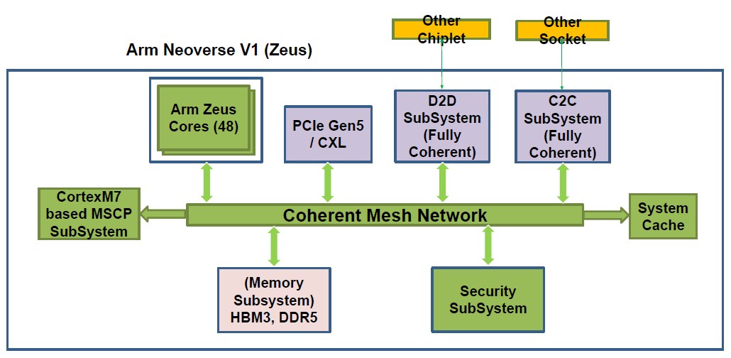
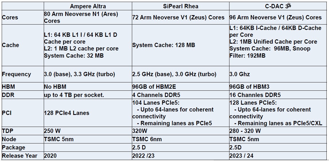
As you would possibly anticipate, C-DAC has chosen the “Zeus” Neoverse V1 cores from Arm Holdings, and is placing 48 of them on a package deal. We don’t know whether it is utilizing a chiplet structure, however this A48Z chip, as it is usually known as, seems like a monolithic design, as you’ll be able to see from the diagram beneath.
The reminiscence subsystem on the A48Z helps each eight channels of DDR5 reminiscence operating at a most of 5.2 GHz and has a pair of HBM3 reminiscence controllers operating at 6.4 GHz which are being geared down to five.6 GHz within the preliminary launch. The HBM3 reminiscence scales as much as 64 GB per dual-chiplet package deal, which isn’t an enormous quantity of reminiscence however which is augmented by the DDR5 reminiscence. Like this:
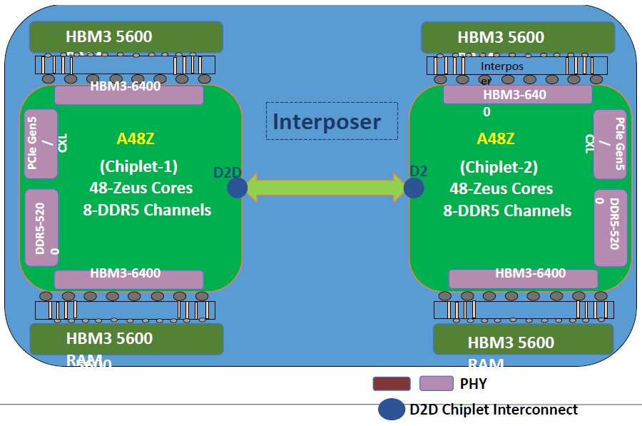
The Aum package deal will embrace a pair of those 48-core chiplets linked to one another utilizing a die-to-die (D2D) interconnect, which is totally coherent.
Nvidia is doing a buyer Arm V9 core design for the Grace CPU, whereas C-DAC and AWS are sticking with the inventory Neoverse V1 cores on the Arm V8.4-A stage of their respective Graviton3/3E and Aum designs. The two chiplet Aum CPU package deal has a complete of 96 cores, with 96 MB of L2 cache throughout these cores and one other 96 MB system-level cache shared throughout the cores and buffering between the DDR5 and HBM3 recollections and the L2 caches.
In addition to the D2D interconnect, there may be one other chip-to-chip interconnect (C2C) primarily based on the CCIX protocol created by Xilinx and endorsed by Arm Holdings, which can permit for a number of packages to be linked to one another NUMA-style with full reminiscence coherency. It isn’t clear how far that CCIX NUMA could be pushed, however two sockets is a minimal and has been revealed, however assist for 4 sockets is probably going for giant reminiscence server footprints in some unspecified time in the future, and eight sockets is completely attainable if the C2C interconnect has sufficient lanes. Each Aum chiplet has 64 lanes of PCI-Express 5.0 connectivity, for a complete of 128 lanes, and we predict that 64 of these lanes are eaten to supply the NUMA hyperlinks primarily based on the CCIX protocol between two Aum sockets, similar to AMD does with its Epyc processors utilizing the Infinity Fabric protocol.
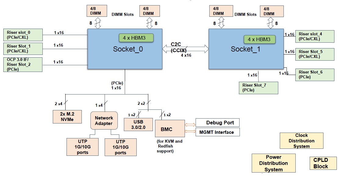
C-DAC says that an Aum node, presumably with two CPUs, will ship round 10 teraflops of peak compute. A two-socket Aum server could have sufficient bandwidth so as to add 4 GPU accelerators.
We have no idea if the coherent mesh that hyperlinks the cores to the controllers on the A48Z chiplet is licensed from Arm Holdings or is homegrown. It might be licensed from Arm Holdings.
It seems just like the Aum processor could have a base clock pace of three GHz, with a turbo enhance pace up over 3.5 GHz. With 16 channels of DDR5 reminiscence delivering 332.8 GB/sec of bandwidth and the 64 GB of HBM3 reminiscence (two 16 GB stacks per A48Z chiplet) delivering 2.87 TB/sec, the Aum package deal will ship greater than 4.6 teraflops per socket and three TB/sec of mixture reminiscence bandwidth, for a powerful 0.7 bytes per flops.
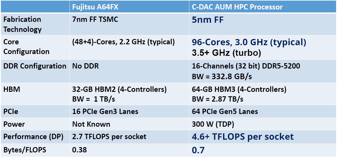
All of this in a 300 watt thermal design level. The Fugaku’s A64FX processor, HBM2 reminiscence, and Tofu D interconnect weigh in at round 170 watts. That Fugaku system has superior vitality effectivity metrics.
Here is an fascinating chart that Wandhekar threw into the deck:
We would have added Graviton2 and Graviton3 in addition to the forthcoming Ampere Computing AmpereOne processor, which can very probably beat the pants off all of those chips on many metrics. When we all know extra, we are going to construct such a desk for you.
[adinserter block=”4″]
[ad_2]
Source link